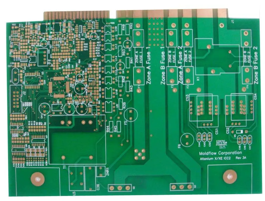
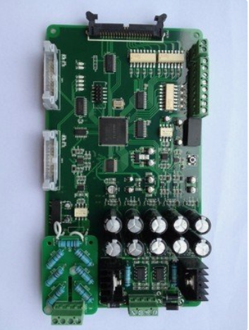
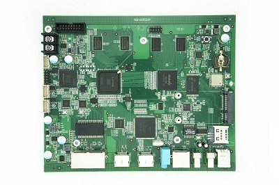
Wiring arrangement and reasonable layout of components on PCB
Introduction to the wiring arrangement and reasonable layout of PCB devices on the PCB board

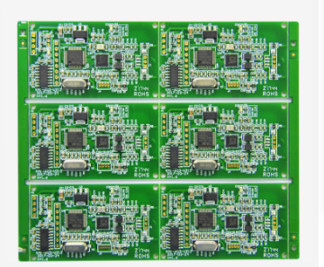
Introduction to the wiring arrangement and reasonable layout of PCB devices on the PCB board

一、PCB覆铜板随着电子产品向轻、薄、小、高密度、多功能方向发展,印制电路板上元器件的组装密度和集成度越来越高,功耗也越来越高, 对PCB基板的散热要求越来越迫切。 如果基板散热不好,会导致印刷电路板...
This article is about the introduction of PCB CCL board level in the production of PCB companies
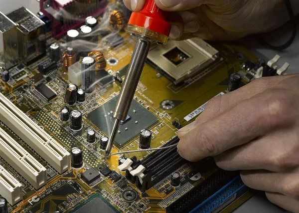
PCBA proofing is the most frequently asked question in our customer consultation. Can you make sampl...
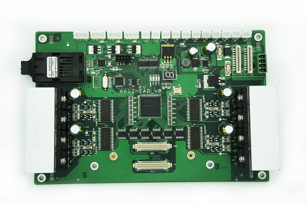
PCBA proofing refers to the trial production of printed circuit boards before mass production. It is...
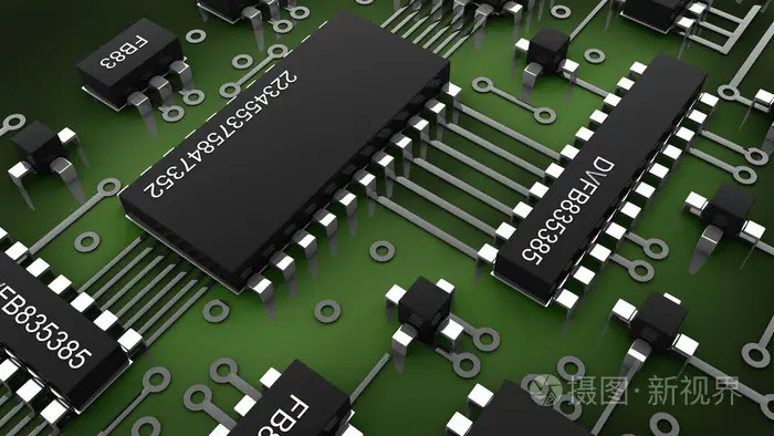
Did you know that almost every gadget or electronic device you use in your daily life has a basic co...
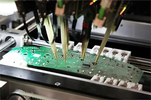
SMT machining technology has become a major application field of SMT process, and different processe...
印刷电路板将金属层置于单独的布线层上,因此各层之间的从属连接必不可少。 为了达到层间连接的目的,需要采用错孔的方法形成通路,并在孔壁上做成可靠的导体,才能完成电气或信号的连接。 自通孔电镀问世以来,几...

高密度印刷电路板是由绝缘材料辅以导体布线形成的结构部件。 最终产品中安装了集成电路、晶体管、二极管、无源元件(如电阻器、连接器等)和各种其他电子元件。 通过导线连接可以形成电信号和功能。 因此,印刷电...

抖音二维码

Q Q二维码

微信二维码
电话热线
13410863085Q Q

微信